The Circuit Board Assembly Process
Circuit Board Assembly Process
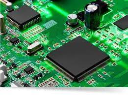
Printed circuit boards (PCB) are more common than you might think, being present in the majority of electronic devices we use every day. The PCB itself is a crucial component that ensures all of the components in your device function properly, which makes it important to have a solid understanding of how circuit board assembly works.
The first step in the circuit board assembly process is stenciling, where solder paste is applied to the bare PCB. This is done by using a stainless-steel stencil with openings that correspond to where the components will be placed on the finished PCB. The assembler then uses a mechanical fixture to hold the stencil and applicator in place while the solder paste is applied.
Next, the assembler places the components onto the PCB using a pick-and-place machine. The assembler can choose to use Surface Mount Technology (SMT) or Through-Hole Technology (THT). SMT is characterized by components with small, flat contacts that are mounted directly on the surface of the PCB, while THT requires component leads to be inserted into holes on the copper PCB traces and soldered in place. The assembler can also opt to use Mixed Technology, which leverages the strengths of both SMT and THT.
The Circuit Board Assembly Process
After the components are positioned on the PCB, it goes through the reflow soldering process. This process consists of three zones: the preheat zone, the ramp-up zone, and the reflow zone. In the preheat zone, the PCB is heated to a temperature that activates the flux in the solder paste and removes any moisture. Then, the reflow zone heats the board to the reflow temperature, which melts the solder paste and bonds it to the component pads.
During the reflow process, the assembler may need to perform additional soldering operations to make sure the connections between the components are strong and secure. Once the reflow is complete, the assembler can inspect and test the circuit board for quality.
As a designer, you can help to improve the circuit board assembly process by adhering to Design for Manufacture (DFM) and Design for Assembly (DFA) principles. This includes making your schematic diagram clear and concise, arranging components to maximize signal flow and minimize interference, and by addressing thermal concerns. It’s also a good idea to incorporate silkscreen markings and labels that clearly indicate components, connectors, and reference designators.
Finally, before sending your circuit board out for assembly, you should run a Design Rule Check to ensure the board meets all manufacturing requirements. This can prevent issues during the reflow and soldering processes, which can lead to costly mistakes and delays in production time.
With the right knowledge, you can work with your assembler to optimize the circuit board assembly process and ensure that the end product is of high quality. This is why it’s so vital to maintain open lines of communication with your assembler throughout the entire process.